- 您现在的位置:买卖IC网 > Sheet目录472 > MAX2121EVKIT# (Maxim Integrated)KIT EVAL FOR MAX2121
�� �
�
�Complete� Direct-Conversion� L-Band� Tuner�
�Pin� Description� (continued)�
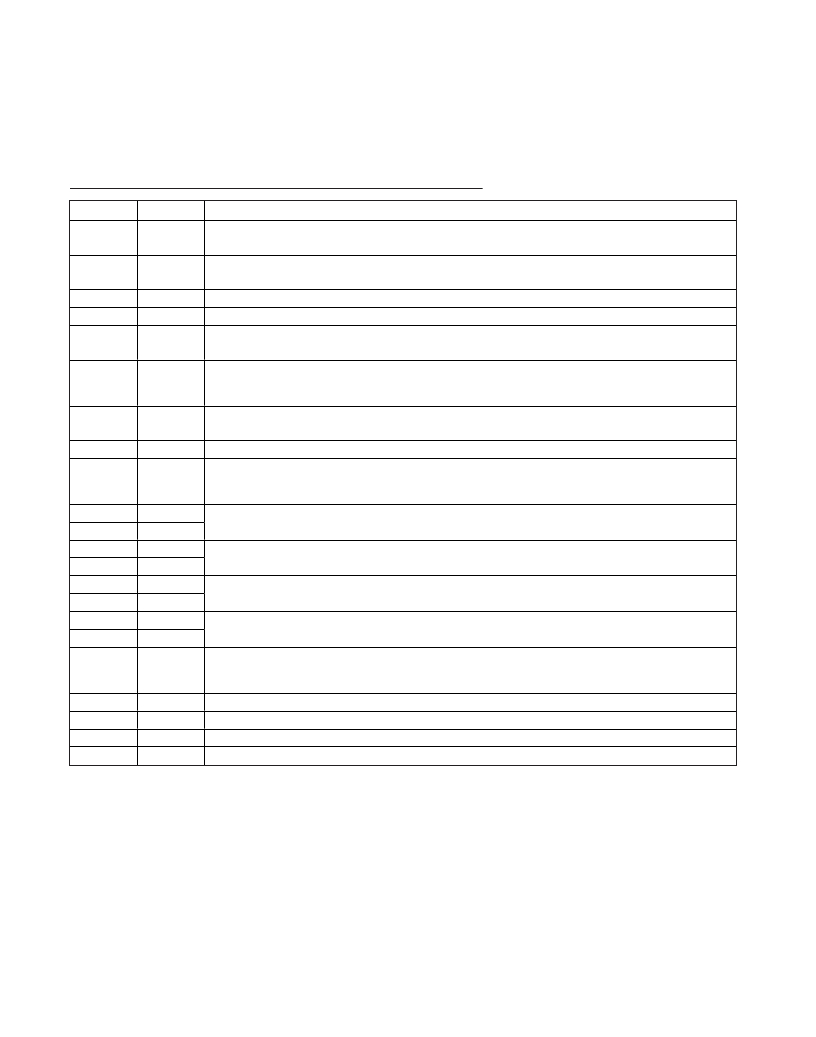
�PIN�
�8�
�9�
�10�
�11�
�12�
�13�
�14�
�15�
�16�
�17�
�18�
�19�
�20�
�21�
�22�
�23�
�24�
�25�
�NAME�
�BYPVCO�
�TUNEVCO�
�GNDTUNE�
�GNDSYN�
�CPOUT�
�V� CC_SYN�
�XTAL�
�REFOUT�
�V� CC_DIG�
�QOUT+�
�QOUT-�
�IOUT+�
�IOUT-�
�IDC+�
�IDC-�
�QDC+�
�QDC-�
�V� CC_BB�
�FUNCTION�
�Internal� VCO� Bias� Bypass.� Bypass� to� GND� with� a� 100nF� capacitor� connected� as� close� as� possible� to�
�the� pin.� Do� not� share� capacitor� ground� vias� with� other� ground� connections.�
�High-Impedance� VCO� Tune� Input.� Connect� the� PLL� loop� filter� output� directly� to� this� pin� with� as� short� of�
�a� connection� as� possible.�
�Ground� for� TUNEVCO.� Connect� to� the� PCB� ground� plane.�
�Ground� for� Synthesizer.� Connect� to� the� PCB� ground� plane.�
�Charge-Pump� Output.� Connect� this� output� to� the� PLL� loop� filter� input� with� the� shortest�
�connection� possible.�
�DC� Power� Supply� for� Synthesizer� Circuits.� Connect� to� a� +3.3V� low-noise� supply.� Bypass� to� GND� with�
�a� 1nF� capacitor� connected� as� close� as� possible� to� the� pin.� Do� not� share� capacitor� ground� vias� with�
�other� ground� connections.�
�Crystal-Oscillator� Interface.� Use� with� an� external� parallel-resonance-mode� crystal� through� a� series�
�1nF� capacitor.� See� the� Typical� Application� Circuit� .�
�Crystal-Oscillator� Buffer� Output.� A� DC-blocking� capacitor� must� be� used� when� driving� external� circuitry.�
�DC� Power� Supply� for� Digital� Logic� Circuits.� Connect� to� a� +3.3V� low-noise� supply.� Bypass� to� GND� with�
�a� 1nF� capacitor� connected� as� close� as� possible� to� the� pin.� Do� not� share� capacitor� ground� vias� with�
�other� ground� connections.�
�Quadrature� Baseband� Differential� Output.� AC-couple� with� 47nF� capacitors� to� the� demodulator� input.�
�In-Phase� Baseband� Differential� Output.� AC-couple� with� 47nF� capacitors� to� the� demodulator� input.�
�I-Channel� Baseband� DC� Offset� Correction.� Connect� a� 47nF� ceramic� chip� capacitor� from� IDC-� to� IDC+.�
�Q-Channel� Baseband� DC� Offset� Correction.� Connect� a� 47nF� ceramic� chip� capacitor� from� QDC-� to� QDC+.�
�DC� Power� Supply� for� Baseband� Circuits.� Connect� to� a� +3.3V� low-noise� supply.� Bypass� to� GND� with�
�a� 1nF� capacitor� connected� as� close� as� possible� to� the� pin.� Do� not� share� capacitor� ground� vias� with�
�other� ground� connections.�
�26�
�27�
�SDA�
�SCL�
�2-Wire� Serial-Data� Interface.� Requires�
�2-Wire� Serial-Clock� Interface.� Requires�
�1k�
�1k�
�pullup� resistor� to� V� CC� .�
�pullup� resistor� to� V� CC� .�
�28�
�—�
�ADDR�
�EP�
�Address.� Must� be� connected� to� either� ground� (logic� 0)� or� supply� (logic� 1).�
�Exposed� Pad.� Solder� evenly� to� the� board’s� ground� plane� for� proper� operation.�
�9�
�发布紧急采购,3分钟左右您将得到回复。
相关PDF资料
MAX2130EVKIT
EVAL KIT MAX2130
MAX2140EVKIT
EVAL KIT MAX2140
MAX2150ETI+T
IC MODULATOR I/Q WIDE 28TQFN
MAX2160EVKIT
EVAL KIT MAX2160
MAX2163ETI/V+
IC TUNER ISDB-T LOW IF 28TQFN
MAX2165EVKIT+
KIT EVAL FOR MAX2165
MAX2170EVKIT+
KIT EVAL FOR MAX2170
MAX2202EWT+T
IC POWER DETECTOR RMS 6-WLP
相关代理商/技术参数
MAX212C/D
功能描述:RS-232接口集成电路 +3V Powered Low-Power True RS-232 Transceiver RoHS:否 制造商:Exar 数据速率:52 Mbps 工作电源电压:5 V 电源电流:300 mA 工作温度范围:- 40 C to + 85 C 安装风格:SMD/SMT 封装 / 箱体:LQFP-100 封装:
MAX212CAG
功能描述:RS-232接口集成电路 RoHS:否 制造商:Exar 数据速率:52 Mbps 工作电源电压:5 V 电源电流:300 mA 工作温度范围:- 40 C to + 85 C 安装风格:SMD/SMT 封装 / 箱体:LQFP-100 封装:
MAX212CAG+
功能描述:RS-232接口集成电路 3V True RS-232 Transceiver RoHS:否 制造商:Exar 数据速率:52 Mbps 工作电源电压:5 V 电源电流:300 mA 工作温度范围:- 40 C to + 85 C 安装风格:SMD/SMT 封装 / 箱体:LQFP-100 封装:
MAX212CAG+T
功能描述:RS-232接口集成电路 3V True RS-232 Transceiver RoHS:否 制造商:Exar 数据速率:52 Mbps 工作电源电压:5 V 电源电流:300 mA 工作温度范围:- 40 C to + 85 C 安装风格:SMD/SMT 封装 / 箱体:LQFP-100 封装:
MAX212CAG-T
功能描述:RS-232接口集成电路 RoHS:否 制造商:Exar 数据速率:52 Mbps 工作电源电压:5 V 电源电流:300 mA 工作温度范围:- 40 C to + 85 C 安装风格:SMD/SMT 封装 / 箱体:LQFP-100 封装:
MAX212CWG
功能描述:RS-232接口集成电路 RoHS:否 制造商:Exar 数据速率:52 Mbps 工作电源电压:5 V 电源电流:300 mA 工作温度范围:- 40 C to + 85 C 安装风格:SMD/SMT 封装 / 箱体:LQFP-100 封装:
MAX212CWG-T
功能描述:RS-232接口集成电路 RoHS:否 制造商:Exar 数据速率:52 Mbps 工作电源电压:5 V 电源电流:300 mA 工作温度范围:- 40 C to + 85 C 安装风格:SMD/SMT 封装 / 箱体:LQFP-100 封装:
MAX212EAG
功能描述:RS-232接口集成电路 RoHS:否 制造商:Exar 数据速率:52 Mbps 工作电源电压:5 V 电源电流:300 mA 工作温度范围:- 40 C to + 85 C 安装风格:SMD/SMT 封装 / 箱体:LQFP-100 封装: